| |
| About Us |
| Services |
| Investors |
| Careers |
| Contact Us |
| Back to Home |
![]()
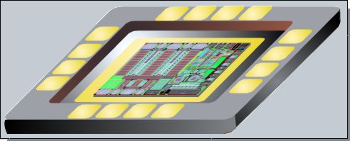
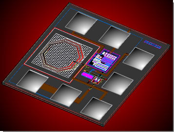
| Application Specific Integrated Circuits |
|
Application Specific Integrated Circuits or ASIC require special training to acquire the expertise. For designing, fabricating and testing an ASIC, very little or no literature is available at times. This is a major setback for startup companies with limited workforce and average experience. No training institutes are available for such a training and industries treat such a design flow as Confidential Intellectual Property. For the very first time we have undertaken this task to make such technology information available to all industries and academic institutions alike. Not only that, depending on your interest we walk you through the complete product development cycle up to packaging and testing. Workshops are organized into chapter with appropriate theory and practical coverage. Each workshop is a tested design flow in Agilent's Advanced Design System. Please have a look at our catalogue and choose the workshops. Kindly fill out our request form for the workshop you are interested in, providing us your exact requirements. Our representatives can approach you with a quick quotation and schedule a customized workshop if required. |
Linear Power Amplifier Design Principles and Practices
Aim of the workshop: To explain various specifications of a Linear Power Amplifier, illustrate design flow in Agilent's ADS, discuss various matching topologies, linearity considerations, efficiency trade-offs, demonstrate a design technique with guaranteed first pass success using powerful ADS EM Co-simulation and Ptolemy Co-simulation Environments. Duration of the workshop: 3 Days Outline of the workshop: Through this workshop- a) We will see specifications of a Linear Power Amplifier in various modern communication systems like IS95 CDMA, UMTS WCDMA 3GPP, WiFi IEEE 802.11a/b/g, WiMAX IEEE 802.16d/e. We will also see the spectral characteristics of modulated signal generated from ADS Ptolemy Signal Sources. b) We will learn about compression characteristics of a device with different biasing schemes, non-linearity like harmonic distortion, inter-modulation distortion, AM-to-AM and AM-to-PM Conversion and look at spectral characteristics of modulated signal before and after amplification. c) We will capture the board ground effects using EM Simulation and use them in our designs. d) We will demonstrate biasing techniques for transistors, design and simulate bias de-coupling circuit using ADS Momentum, fit the SPICE Model for bias decoupling circuit for use in circuit simulations. e) We will perform small signal matching, observe impedance movement with self biasing, optimize match for large signal, and finally perform load pull to plot constant gain, PAE and ACPR contours to validate our match and refine it f) We will learn to design temperature compensated bias circuit, explain mode control circuit design, design power detector for power control loop. g) We will perform single tone and two tone simulations in ADS Harmonic Balance and plot Intermodulation Products versus power for the designed Power Amplifier. h) We will use modulated signal sources from ADS Ptolemy to perform Envelope Simulations on the designed Power Amplifier and plot ACPR Characteristics. We will discuss spectral masks for modulation schemes. i) We will compute Percentage EVM Characteristics of the Power Amplifier with OFDM Signals as input, plot Data Constellation before and after amplification. j) We will layout the amplifier and capture the parasitics using EM Co-simulation Flow. Pre-requisite: ADS Fundamental Training Course Number: LINPA300NC To express your desire to undertake this workshop, kindly fill in Request FormClass E High Efficiency Power Amplifier Design Principles
Aim of the workshop: To explain the concept of high efficiency amplification, introduce the commercial areas where high efficiency amplification is required, describe the principle of operation of Class E Amplifier, introduce various class E topologies, derive design equations and numerically solve them, and walk through the designs of lumped and distributed Class E Amplifiers. Duration of the workshop: 2 Days Outline of the workshop: Through this workshop- a) We will discuss various applications where Class E Amplification may be required. b) We will introduce the concept of achieving 100% Power Added Efficiency of a Power Amplifier. We will derive the characteristic equations for such an amplification. c) We will present design equations for Class E Amplifier at any load quality factor and switching duty cycle. d) We will discuss the stress on a power device and the safe operating conditions. e) We will discuss losses in a power device that lead to PAE slightly less than 100%. f) We will design a MMIC Class E amplifier using on-chip lumped components and a MIC Class E Amplifier using distributed components. Pre-requisite: ADS Fundamental Training Course Number: CLEPA200NC To express your desire to undertake this workshop, kindly fill in Request Form
Low Noise Amplifier Design Principles and Practices
Aim of the workshop: To explain various specifications of a Low Noise Amplifier, illustrate design flow in Agilent's ADS, discuss various matching topologies, simulate noise figure and deal with noise sources to minimize noise, linearity considerations (input -1dB Compression Point), quiescent current trade-offs, demonstrate a design technique with guaranteed first pass success using powerful ADS EM Co-simulation and Ptolemy Co-simulation Environments. Duration of the workshop: 2 Days Outline of the workshop: Through this workshop- a) We will see specifications of a Low Noise Amplifier in various modern communication systems like IS95 CDMA, UMTS WCDMA 3GPP, WiFi IEEE 802.11a/b/g, WiMAX IEEE 802.16d/e. We will discuss sensitivity and dynamic range of a receiver for various systems. b) We will learn about noise sources in a transistor circuit that contribute to noise. We will also highlight the role of grounding and substrate vias in noise contribution.We will observe the effect of source degeneration on input match and minimum noise figure. c) We will learn about compression characteristics of a device with different biasing schemes, non-linearity like harmonic distortion, inter-modulation distortion etc. d) We will capture the board ground effects using EM Simulation and use them in our designs. e) We will demonstrate low noise biasing techniques for transistors, design and simulate bias de-coupling circuit using ADS Momentum, fit the SPICE Model for bias decoupling circuit for use in circuit simulations. f) We will perform small signal matching, observe impedance movement with self biasing, optimize match for large signal and adjust input compression point. g) We will learn to design temperature compensated bias circuit. h) We will perform single tone and two tone simulations in ADS Harmonic Balance and plot Intermodulation Products versus power for the designed Low Noise Amplifier. i) We will layout the amplifier and capture the parasitics using EM Co-simulation Flow. Pre-requisite: ADS Fundamental Training Course Number: VPLNA200NC To express your desire to undertake this workshop, kindly fill in Request FormMMIC Design Flow and Techniques Using Agilent ADS
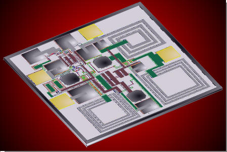
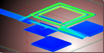
Aim of the workshop: To demonstrate a verified MMIC Design Flow in Agilent's ADS guanateed for a first pass success for various MMIC Designs, to explain the basic microwave theory involved in passive and active circuit design, describe a methodology to model passive MMIC components, boards, gain stages etc., walk though with examples on small signal and large signal designs, and introduce the design of experiment to improve yield. Duration of the workshop: 3 Days Outline of the workshop: Through this workshop- a) We will brush up your microwave basics - maxwell's equations, constitutive relations, material properties, solution of maxwell's equations etc. b) We will apply microwave basics to study transmission lines and field solution. c) We will design various forms of transmission lines using Agilent's ADS, layout and EM Simulate them in MOMENTUM to verify our design. d) We will study network parameters, their meaning, inter-conversion and application to model circuits. e) We will design on-chip spiral inductors and MIM capacitors in MOMENTUM, EM Simulate them and fit SPICE models using network parameters. f) We will discuss DC and RF characteristics of an active device. We will explain voltage and power amplification concepts. g) We will design and EM simulate a bias decoupling circuit. We will appropriately bias a transistor and do a small signal match to achieve modest return losses. h) We will analyze the stability of a gain stage and suggest various ways of stabilizing a circuit. i) We will discuss various temperature compensated bias circuits in MMIC and Bi-CMOS Processes. j) We will perform Harmonic Balance Simulation on the gain stage to plot, gain, compression characteristics, return losses, PAE and match movement with input power. k) We will perform Envelope Simulation using actual modulated signals and plot ACPR for the gain stage. l) We will simulate yield, perform sensitivity analysis, and improve the yield using Design Of Experiments. Pre-requisite: ADS Fundamental Training Course Number: MMICE300NC To express your desire to undertake this workshop, kindly fill in Request Form Voltage Controlled Oscillator Design Principles and Practices
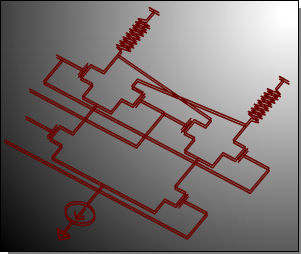
Aim of the workshop: To discuss the principle of operation of VCO, present two types of oscillators, explain phase noise and its sources in a VCO circuit, discuss ways to improve phase noise of a VCO, discuss layout issues in order to optimize phase noise and to walk through the design, layout and simulation of a VCO in Agilent's ADS. Duration of the workshop: 2 Days Outline of the workshop: Through this workshop- a) We will present the principles of operation of a MMIC and a Differential CMOS VCO. b) We will discuss phase noise in two topologies. c) We will design a VCO core. d) We will discuss two oscillator port phase noise measurement technique. e) We will simulate phase noise of the designed differential VCO. f) We will discuss design trade-offs and optimize phase noise. g) We will design PTAT and Bandgap referenced bias. h) We will layout the VCO and perform EM Co-simulations. Pre-requisite: ADS Fundamental Training Course Number: LPVCO200NC To express your desire to undertake this workshop, kindly fill in Request Form Antenna Design Theory and Practices
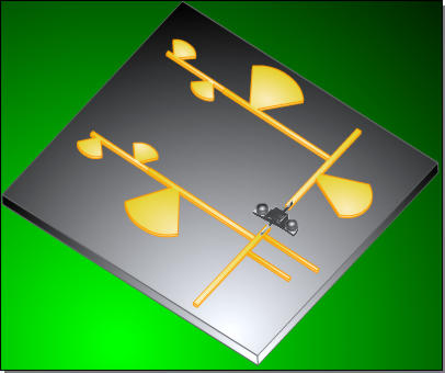
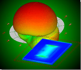
Aim of the workshop: To present the role of antenna as a matching and radiation element, introduce various forms of antenna, discuss radiation mechanisms, show radiation patterns and define radiation properties, present methods to design patch antennas and arrays. Duration of the workshop: 3 Days Outline of the workshop: Through this workshop- a) We will discuss the role of antenna as matching and radiation element b) We will see various antenna structures. c) We will discuss radiation mechanisms using maxwell's equations. d) We will see radiation patterns and define various radiation properties. e) We will derive and plot field configuration in resonant structures. f) We will discuss antenna feed mechanisms and matching. g) We will design microstrip patch antennas and simulate its pattern. h) We will discuss design procedure for N-element antenna array. i) We will discuss design procedure for aperture antennas j) We will study antenna measurement techniques. Pre-requisite: ADS Fundamental Training Course Number: BANTE300NC To express your desire to undertake this workshop, kindly fill in Request Form Mixer Design Theory and Practices
Aim of the workshop: To present the theory of mixing, discuss FET and Bipolar versions of Gilbert Cell Mixer, derive the conversion gain, discuss design equations and walk through the design of High Input Dynamic Range and High Conversion Gain Gilbert Cell Mixer. Duration of the workshop: 1 Day Outline of the workshop: Through this workshop- a) We will discuss mixer theory and principle of operation b) We will present FET and Bipolar Gilbert Cell Mixers and derive conversion gain equations. c) We will walk through the design of FET Gilbert Cell Mixer for large input dynamic range and large conversion gain. Pre-requisite: ADS Fundamental Training Course Number: TMIXE100NC To express your desire to undertake this workshop, kindly fill in Request Form |